|
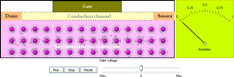
1. Field Effect Transistor:
The field-effect transistor (FET) is a type of transistor that utilizes an electric field to control
the shape of a channel in which charge carriers in a semiconductor material flow. When the channel
narrows down, the current in the channel diminishes. When the channel opens up, the current increases.
The FET is an important building block of integrated circuits. This interactive model shows how the
FET works.
|
|
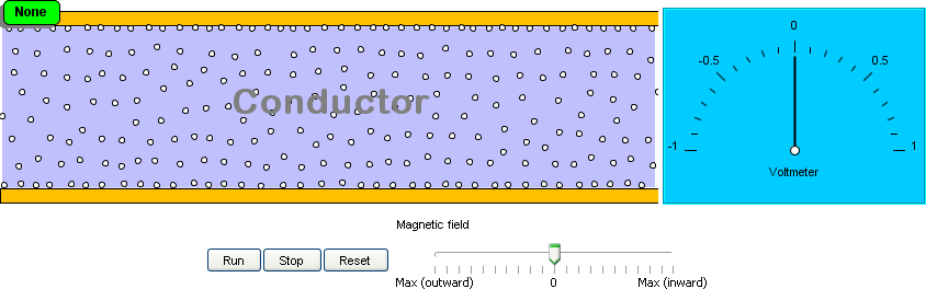
2. The Hall effect:
When an electric current flows in a conductor in the presence of a magnetic field, a voltage is detected across
the conductor. This is called the Hall effect. The Hall effect is used to design sensors that measure rotational
speed, fluid flow, pressure, and so on. This model shows the Hall effect.
|
|
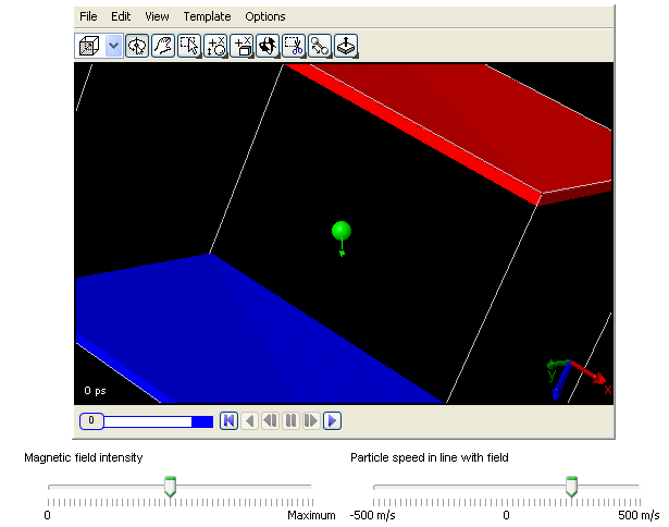
3. The Lorentz force:
When a charged particle moves in an electromagnetic field, it experiences a force called the Lorentz force. The Lorentz
force is propotional to the charge and the speed of the particle, but is always perpendicular to the direction of
the magnetic field and the velocity. You can learn how a charged particle moves under this force using this 3D
model.
|
|
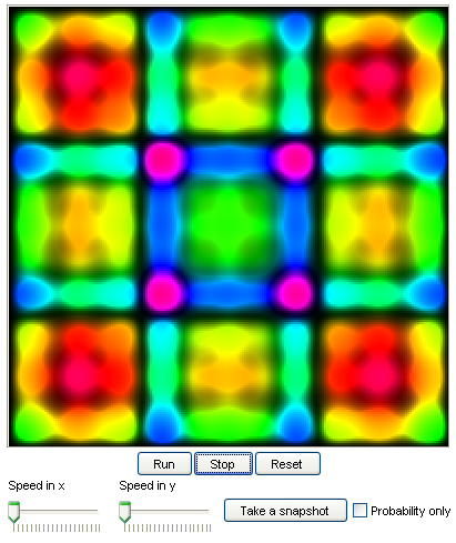
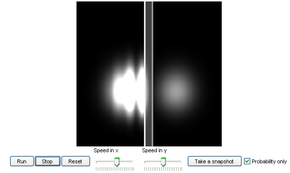
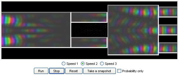
4. Quantum motion in a box:
This model shows how a wave packet, which represents a quantum particle, evolves when it is placed inside
a box. Students can experiment with a few other different setups in the box.
|
|
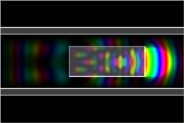
5. Quantum tunneling effect:
Electrons moving against a potential energy barrier
can penetrate through the barrier, even if their kinetic energy is not high enough to surmount
the energy barrier. This is known as the quantum tunneling effect. This is very important in
microscopic imagery, semiconductor devices, and chemistry.
|
|
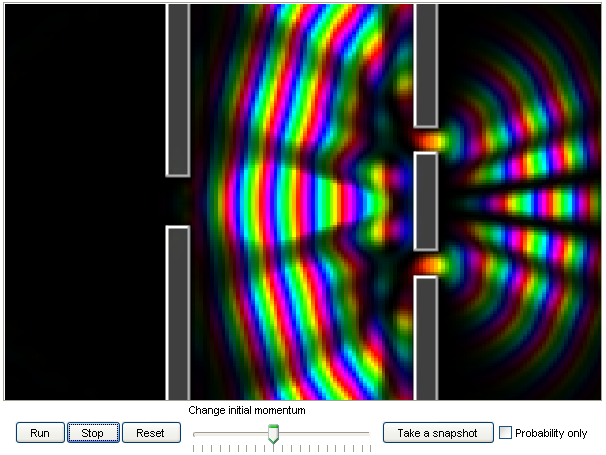
6. Electron diffraction in a double-slit experiment:
Electrons act like waves. In this double-slit experiment, you can shoot an electron at a double-slit
with different speeds, and observe the diffraction patterns.
|
|
7. Quantum well:
Quantum wells are structures in semiconductors that can confine electrons within an area. Quantum wells
can be used to produce laser.
|
|
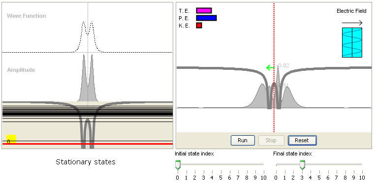
8. Radioactive transitions:
This model demonstrates how radioactive transitions (photon absorption and stimulated emission) occur in
an optical field. Many important phenonmena are emergent behaviors of this dynamic model. For example,
it shows that it is the frequency, not the intensity, of the incident light that determines whether or not
the transition will happen. It also shows the transitions are forbidden between some states.
|
|
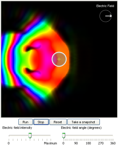
9. Polarization:
This model demonstrates how an electron cloud shifts to cause an atom to be polarized.
|
|
10. Covalent bonding:
This model demonstrates when two nuclei are close enough, electrons move around both of them and form
a covalent bond.
|
|
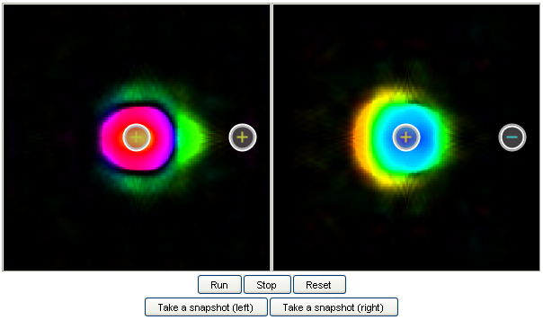
11. Ionization:
This model demonstrates how the electron is ionized when a static electric field is applied. You can
see that there is some degree of ionization even when the field is not very strong. This is known as
tunnel ionization (in which the electron tunnels through the confining potential from the atom and
escape).
|
|
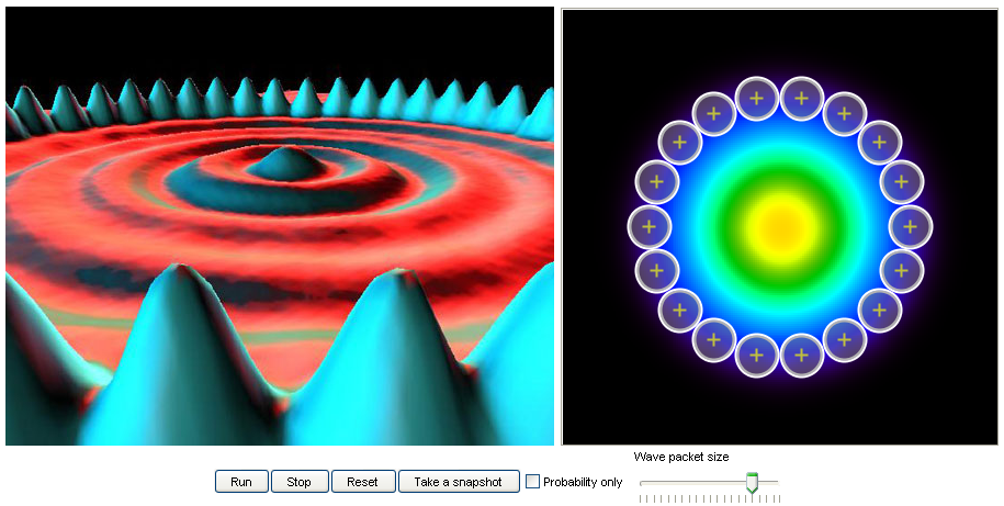
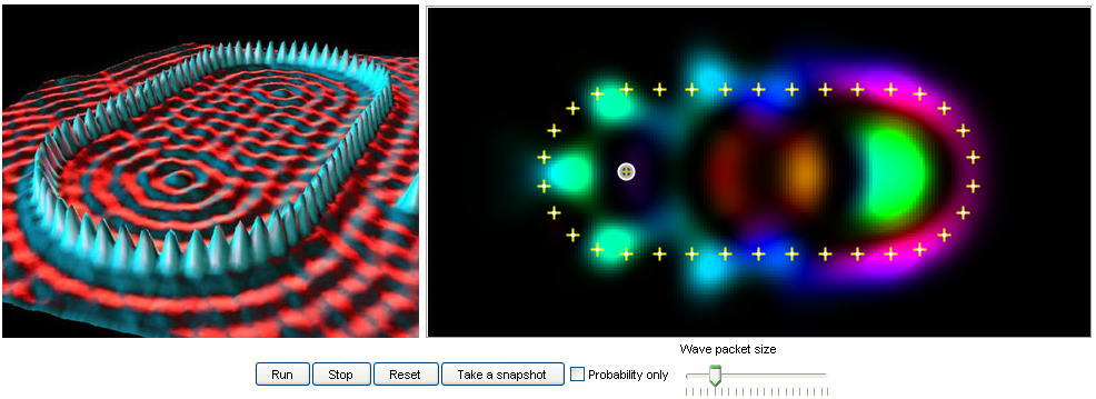
12. Quantum corral:
Left: An STM image of a quantum corral made of iron atoms on a copper (111) surface
(http://www.almaden.ibm.com/vis/stm/corral.html).
Right: A 2D quantum dynamics simulation that shows the motion of an electron cloud in a corral setup.
|
|
13. Quantum mirage:
When scientists placed an atom at one focus of a stadium quantum corral, a mirage of the atom appeared at
the other focus. Specifically the same electronic properties were present in the electrons surrounding both
foci, even though the atom was only present at one focus. The electron cloud around the other focus is
called quantum mirage, a phenomenon scientists hope to construct atomic-scale processors in the future. |
|
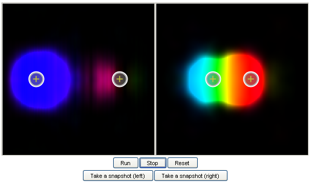
14. An electronic star coupler:
A star coupler is a device that takes in an input signal and splits it into several output signals.
This model is a design of a nanoscale electronic star coupler that can split an input electric signal
into three outputs for an electric wave packet that travels at certain speeds. |
|
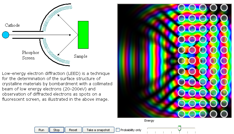
15. Low-energy electron diffraction (LEED):
LEED is a technique for the determination of the surface structure of
crystalline materials by bombardment with a collimated beam of low energy electrons (20-200eV)
and observation of diffracted electrons as spots on a fluorescent screen. This model shows
how it works and why the energy of the electron matters. |